Wisconsin Parts Database Instructions and Discussion Team/Group > WISCONSIN
> Motors and tools
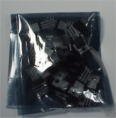
> (25) NDP7060L n-channel field effect transistors to-220
(25) NDP7060L n-channel field effect transistors to-220
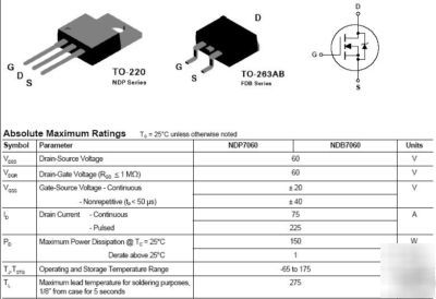
N-Channel Enhancement Mode Field Effect Transistor
General Description Features http://www.datasheetcatalog.org/datasheet/nationalsemiconductor/DS013094.PDF
75A, 60V. RDS(ON) = 0.013W @ VGS=10V.
Critical DC electrical parameters specified at elevated
Rugged internal source-drain diode can eliminate the need
for an external Zener diode transient suppressor.
175 C maximum junction temperature rating.
High density cell design for extremely low RDS(ON).
TO-220 and TO-263 (D2PAK) package for both through hole
and surface mount applications.
Absolute Maximum Ratings TC = 25 C unless otherwise noted
Symbol Parameter NDP7060 NDB7060 Units
VDSS Drain-Source Voltage 60 V
VDGR Drain-Gate Voltage (RGS < 1 MW) 60 V
VGSS Gate-Source Voltage - Continuous 20 V
- Nonrepetitive (tP < 50 s) 40
ID Drain Current - Continuous 75 A
PD Maximum Power Dissipation @ TC = 25 C 150 W
TJ,TSTG Operating and Storage Temperature Range -65 to 175 C
TL Maximum lead temperature for soldering purposes,
1/8" from case for 5 seconds 275 C