Wisconsin Parts Database Instructions and Discussion Team/Group > MICHIGAN
> Machine Parts
> Xilinx virtex-4 LX200 multi-fpga soc plateform
Xilinx virtex-4 LX200 multi-fpga soc plateform
Xilinx Virtex-4 LX200 Multi-FPGA SOC Platform
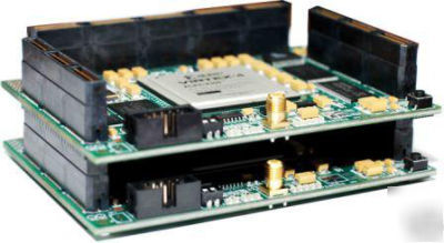
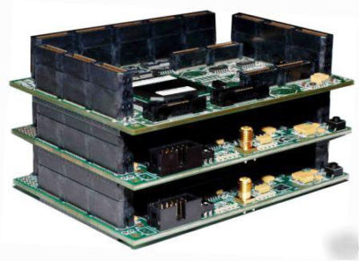
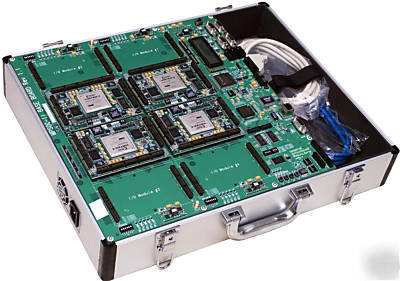
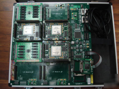
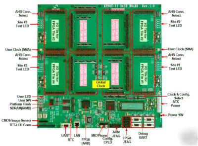
The HTG-MPSOC is an ideal prototyping and evaluation platform for high-end designs requiring high density FPGA devices, processing power, and AMBA AHB interfaces. This Platform enables SoC developers to verify custom IP cores, prototype complete systems, develop and test device drivers for projects. The HTG-MPSOC platform can potentially be populated with 8 Xilinx Virtex-4 LX200 FPGAs and multiple ARM926EJ-S or ARM1136JF-S Core Tile modules (or any other customized DSP or Processor modules). This Platform consists of a "Base" board and multiple "FPGA" Modules.
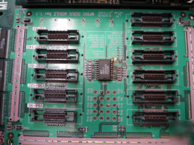
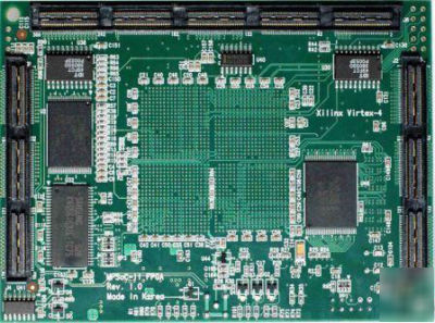
The "Base" board provides power, memory, and standard peripherals used in embedded and wireless applications 64MB SDRAM, CIS, TFT-LCD, AC97 Codec, 10/100 Ethernet, 5 UART ports, User LEDs and Switches. The Base board provides four "Expansion" connectors with 288 signal pins so add-on modules can be connected to the rest of the Base board and FPGA resources. The Base board also has four connectors which provide interfaces to the "FPGA" boards.
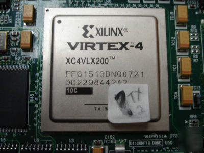
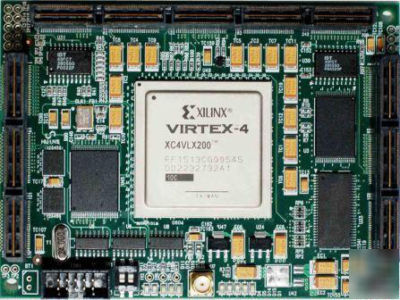
Each compact "FPGA" Module is populated with Xilinx Virtex-4 XC4VLX200-10FF1513 Device, 64MB SDRAM/32MB Flash, 4MB SRAM, 3 ICS307 PLL, JTAG port, on-board regulator, and connectors to host ARM Core Tile for ARM926EJ-S or ARM1136JF-S (or other modules)
The HTG-MPSOC Platform includes example RTL, FPGA bitstream, and example software that works with the CPU Core Tiles. It includes demonstration code and complete environment for evaluating custom IP.
ARM Core Tile Interface connector
Options (should be purchased from ARM)
- Core Tile for ARM926EJ-S (Versatile/CT926EJ-S)
- Core Tile for ARM1136JF-S (Versatile/CT1136JF-S)
XilinX Virtex4 LX200 FF1513 ? Maximum 20 Million Gates
AHB 40MHz (depending on user design)
4~50MHz by PLL, Three ICS307 PLL ICs
Tile Header connectors on top & bottom of each tile
288 interconnection pins to tile above
468 interconnection pins to tile below
Xilinx Platfom Flash (XCF32P * 2)
FPGA is used to expand AMBA AHB peripherals
4~50MHz by PLL, 2 User OSC sockets, 2 User SMA sockets
5 UART (1 UART for FPGA, 4 UART for each FPGA Module)
Xilinx CPLD controls JTAG mode for ARM and FPGA
3 Xilinx JTAG connector for Xilinx ChipScopePro
User selects configuration mode by using 8 pin DIP SW
1 Xilinx Platform Flash for On-Board FPGA
Two 9-pin female-to-female null modem cables
Micro-ATX PC Power Supply 220V/110V AC
ARM RealView ARM926EJ-S Core Tile
ARM RealView ARM1136JF-S Core Tile
640x480 CMOS Image Camera Module
ARM926EJ-S and ARM1136JF-S Core Tiles
The Core Tile for ARM926EJ-S/ARM1136JF-S contains an ARM926EJ-S/ARM1136JF-S processor inside a test chip. The processor s configuration signals and a multiplexed AHB bus are connected to the board s headers, so that systems based on this core can be easily prototyped.
These boards can be stacked together to implement complex custom systems. The CPU core frequency can be adjusted up to 200MHz, but the maximum frequency depends upon the test-chip fitted. Core Tiles cannot be used stand-alone.