Wisconsin Parts Database Instructions and Discussion Team/Group > ILLINOIS
> Machine Parts
> Add
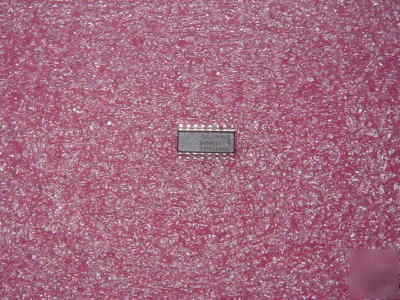
> Qty 10 * 74HC4046 74HC4046AD single pll w/vco smd
Qty 10 * 74HC4046 74HC4046AD single pll w/vco smd
Centre frequency of up to 17 MHz (typ.) at VCC = 4.5 V
Choice of three phase comparators: EXCLUSIVE-OR; edge-triggered JK flip-flop; edge-triggered RS flip-flop
Excellent VCO frequency linearity
VCO-inhibit control for ON/OFF keying and for low standby power consumption
Operating power supply voltage range:
VCO section 3.0 to 6.0 V digital section 2.0 to 6.0 V
Zero voltage offset due to op-amp buffering
The 74HC/HCT4046A are high-speed Si-gate CMOSdevices and are pin compatible with the 4046 of the 4000B series. They are specified in compliance withJEDEC standard no. 7A.The 74HC/HCT4046A are phase-locked-loop circuits thatcomprise a linear voltage-controlled oscillator (VCO) and
three different phase comparators (PC1, PC2 and PC3)with a common signal input amplifier and a commoncomparator input.The signal input can be directly coupled to large voltagesignals, or indirectly coupled (with a series capacitor) tosmall voltage signals.
A self-bias input circuit keeps smallvoltage signals within the linear region of the inputamplifiers. With a passive low-pass filter, the 4046A forms a second-order loop PLL. The excellent VCOlinearity is achieved by the use of linear op-amptechniques.The VCO requires one external capacitor C1 (betweenC1A and C1B) and one external resistor R1 (betweenR1 and GND) or two external resistors R1 and R2(between R1 and GND, and R2 and GND). Resistor R1and capacitor C1 determine the frequency range of theVCO. ResistorR2 enables the VCO to have a frequencyoffset if required.
The high input impedance of the VCO simplifies the designof low-pass filters by giving the designer awide choice ofresistor/capacitor ranges. In order not to load the low-passfilter, a demodulator output of the VCO input voltage isprovided at pin 10 (DEMOUT). In contrast to conventionaltechniques where the DEMOUT voltage is one thresholdvoltage lower than the VCO input voltage, here theDEMOUT voltage equals that of the VCO input. IfDEMOUT is used, a load resistor (RS) should be connectedfrom DEMOUT to GND; if unused, DEMOUT should be left open.
The VCO output (VCOOUT) can be connecteddirectly to the comparator input (COMPIN), or connectedvia a frequency-divider. The VCO output signal has a dutyfactor of 50% (maximum expected deviation 1%), if theVCO input is held at a constant DC level. A LOW level atthe inhibit input (INH) enables the VCO and demodulator,while a HIGH level turns both off to minimize standbypower consumption.The only difference between the HC and HCT versions isthe input level specification of the INH input. This inputdisables the VCO section.
The sections of the comparator are identical, so that there is no difference in theSIGIN (pin 14) or COMPIN(pin 3) inputs between the HCand HCT versions.Phase comparatorsThe signal input (SIGIN) can be directly coupled to theself-biasing amplifier at pin 14, provided that the signalswing is between the standard HC family input logic levels.Capacitive coupling is required for signals with smaller swings.

